Microlens Arrays
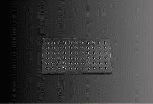
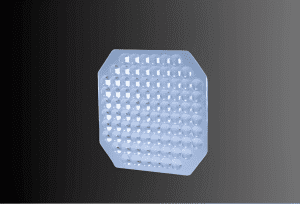
What if you could bring the power of nature’s compound eyes to your optical assembly— in a tiny package 10 mm x 10 mm? It turns out, you can! Whether you need to homogenize light from line-narrowed excimer lasers or high power LEDS, microlens arrays can give you the high efficiency and non-gaussian uniformity you need. These optical assemblies are composed of many tiny micro lenses, arranged in a one or two dimensional array.
Microlens arrays may be produced as separate optical components, and even in mounted form, surrounded by metal or polymer that enables them to fit neatly into an optical mount. They can also be designed to incorporate directly into a larger optical system. Each microlens array may contain thousands or possibly even millions of tiny lenses, arranged to make a square grid, rectangle, or circle.
A microlens array can be characterized by parameters such as focal length, quality of transmitted wavefront, and size. Many microlens arrays are made of UV fused silica, which has high transmission from the UV into the IR range. The fill factor will depend on the specific geometry of the microlenses and the arrangement chosen, but these arrays are typically designed to have a high fill factor to avoid zero-order hotspots. Their optical properties— large field of view angles, low aberration and distortion, infinite depth of field, and high temporal resolution— make them highly desirable for many different applications.
How Microlens Arrays Are Fabricated
Fabricating a microlens array is a little different from traditional lens manufacturing simply because the lenses we are working with are so very small. Typically, all of the microlenses in a microlens array are produced in just one step, and the manufacturing methods used are often adapted from semi conductor processing technology.

One method of fabricating microlens involves photolithography, using a lens pattern defined by a photolithographic mask. Etching techniques are sometimes used, as are hot embossing and printing methods which rely on the surface tension of the liquified substrate. Another manufacturing method involves using laser materials processing, and here sometimes the microlenses are formed individually using multiple processing beams. Laser materials processing offers more versatility than many other methods, but is also more expensive.
Applications of Microlens Arrays
Microlens arrays are often used to homogenize and shape beams, or to collimate the output of fiber arrays. Square array lenses, for instance, might be used in pairs for applications in welding, drilling, fiber coupling and laser ablation. Fly’s eye condenser arrays, which are formed of dual-surface micro cylindrical lenses, are ideal for flat-top and line generation. These arrays are often used when one has a large illuminated field but a very short working distance; for instance, in fluorescence microscopy, semiconductor instrumentation and in applications involving medical lasers.
When used with CCD arrays and CMOS sensors, microlens arrays can collect light that would otherwise have fallen on non-sensitive sensor areas, thus improving efficiency. They are used to focus light for digital projectors and photocopiers.
Microlens arrays can also be integrated into light field cameras, mounted between the main lens and light sensor. This enables the production of a light, compact camera that does not require focus before capturing an image; the focus is chosen during post-processing.
A Shack-Hartmann wavefront sensor is an optical device used to measure the wavefront shape of incident light, often used in adaptive optics. It may be used to determine the wavefront shape of star light, in an optical telescope, or to determine the wavefront in an attenuated laser beam. An important component of the Shack-Hartmann wavefront sensor is a microlens array, which probes the wavefront orientation from many separate points over the cross-section of the beam of light. Essentially what happens is that each of the tiny microlenses focuses the radiation it receives to a spot on the image sensor. Since the position of that spot tells us the orientation of that tiny piece of wavefront, a computer can use the aggregate data from each of the lensless on the microlens array to produce a good estimate of the wavefront distortions.

Other applications of microlens arrays include use as solar concentrators, focusing sunlight to solar cells; in the optical switches and modulators of fiber optical communication systems; in AR and VR imaging systems, and in optical microscopy and spectroscopy.
Custom Microlens Arrays
Are you intrigued by the world of microlens arrays, and would you like to have more information about just how they could be incorporated into your optical system? At Avantier, we specialize in creating custom optics that meet the exact needs of your application— and microlens arrays are one of our areas of expertise. Contact us today if you’d like more information or to set up an initial consult.
GREAT ARTICLE!
Share this article to gain insights from your connections!


